Sensing ApplicationsUnlock the advantages of our Sensing Applications, which are designed to cater to the needs of various industries. As a leading manufacturer, distributor, supplier, trader, and retailer, we offer a range of products that are tailored to meet the requirements of our clients. Our product list includes GFAB - Graphene Foundry Service, GFET-S12 for Sensing applications, GFET-S10 for Sensing applications, GFET-S11 for Sensing applications, and GFET-S20 for Sensing applications. Order our Sensing Applications at the lowest price and experience the extraordinary benefits they offer. Our new release, GFAB - Graphene Foundry Service, is exceptional and is designed to provide the finest results. With over 8.0 years of experience, we have established ourselves as a reliable supplier in the domestic market, catering to All India. We are also an exporter in Asia, providing our clients with the best quality products. Our Sensing Applications are designed to provide exceptional features and advantages. They are highly sensitive and accurate, making them ideal for various sensing applications. They are also easy to use and install, making them a popular choice among our clients. Our products are reliable and durable, ensuring that they provide the best results for a long time. With our Sensing Applications, you can be assured of the finest quality and performance. |
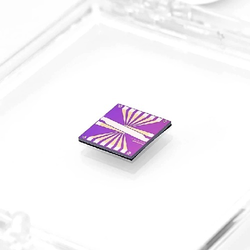
GFET-S20 for Sensing applications
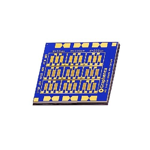
GFET-S10 for Sensing applications
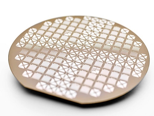
GFAB - Graphene Foundry Service
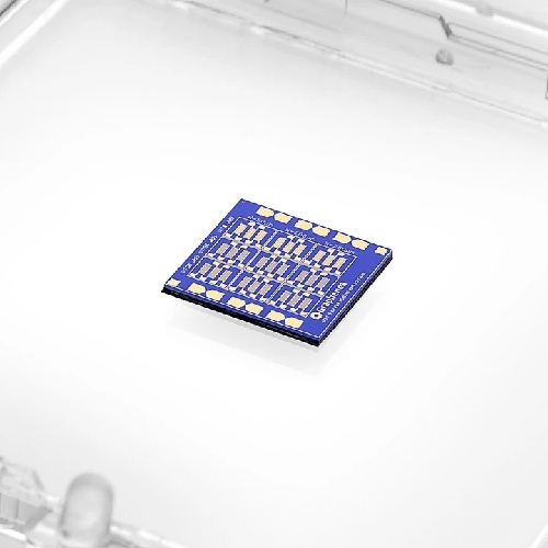
GFET-S12 for Sensing applications
GFET-S11 for Sensing applications
|
|
 |
ULTRANANOTECH PRIVATE LIMITED
All Rights Reserved.(Terms of Use) Developed and Managed by Infocom Network Private Limited. |
