Multilayer CVD Graphene on Nickel Wafer
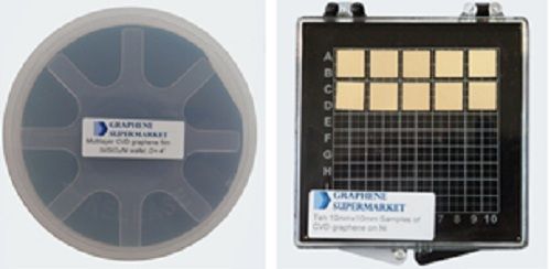
Product Details:
- Size 3-10 microns
- Material Graphene on Nickel Wafer
- Application Graphene on Nickel Wafer
- Chemical Composition Graphene
X
Multilayer CVD Graphene on Nickel Wafer Price And Quantity
Multilayer CVD Graphene on Nickel Wafer Product Specifications
- Graphene on Nickel Wafer
- 3-10 microns
- Graphene on Nickel Wafer
- Graphene
Multilayer CVD Graphene on Nickel Wafer Trade Information
- Paypal
- 4-5 Week
- Seal Packing
- North America Eastern Europe Middle East Asia
- All India
- Technical Data sheets are available upon request
Product Description
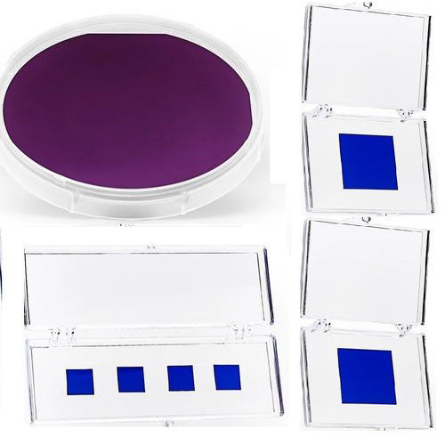
Graphene on nickel is a few monolayers thick, usually between 1-7 layers with an average of 4 monolayer thickness. It looks like a patchwork, whereas each patch has a different thickness. The graphene layers within the same patch are aligned relative to each other (there is a graphitic AB-stacking order). The size of each patch is about 3-10 microns.
Applications:
- Graphene Electronics
- Conductive Coatings
- Aerospace Industry
- Support for Metallic Catalysts
- Microactuators
- MEMS and NEMS
- Chemical and Bio Sensors
- Multifunctional Materials Based on Graphene
- Graphene Research
-
Available Size:
- One Wafer 100mm -4 in
Tell us about your requirement

Price:
Quantity
Select Unit
- 50
- 100
- 200
- 250
- 500
- 1000+
Additional detail
+91
Email
Other Products in 'CVD Films' category
 |
ULTRANANOTECH PRIVATE LIMITED
All Rights Reserved.(Terms of Use) Developed and Managed by Infocom Network Private Limited. |


